SCI论文(www.lunwensci.com)
摘要:制备了一种在p-i-n型AlGaAs/GaAs材料上刻蚀微沟槽的中子探测器。通过MOCVD技术生长了变组分变掺杂的p-i-n型Al⁃GaAs/GaAs,使用ICP技术在材料上刻出微沟槽,沟槽宽度为25µm,深度为10µm。探测器的探测面积为4 mm2,沟槽宽度和间距为1∶1,呈周期性排列,在沟槽中填充中子转换材料探测热中子信号。通过对平面和微结构p-i-n型AlGaAs/GaAs探测器的电学特性、α粒子以及中子探测性能的比较分析,发现两者在电学特性和α粒子能量分辨率方面有较大差别。5 V偏压下平面型和微结构AlGaAs/GaAs探测器的漏电流分别是-0.024 1µA、-0.627µA,两者相差近30倍,这是由于微结构刻蚀了部分异质结导致器件表面漏电流增加。0 V偏压下微结构探测器α粒子能量分辨率比平面型也有些许恶化,但在热中子探测上微结构效果更佳,中子总计数微结构比平面型多一倍。微结构降低了探测器的自吸收问题,同时增大了探测器的中子接触面积,在热中子探测上应用前景广阔。
关键词:AlGaAs,中子探测器,微结构,6LiF,热中子
Performance Characterization of p-i-n AlGaAs/GaAs Microstructure Neutron Detector with Variable Component and Variable Doping
Zhou Qing,Zou Jijun※,Ye Xin,Zhang Mingzhi
(Ministry of Education Engineering Research Center of Nuclear Technology Application,East China University of Technology,Nanchang 330013,China)
Abstract:A neutron detector etching microgrooves on p-i-n AlGaAs/GaAs material had been fabricated.The p-i-n type AlGaAs/GaAs with variable components and variable doping were grown by MOCVD technology,and the micro-grooves with width of 25µm and depth of 10µm were cut into the material by ICP technology.The detection area of the detector was 4 mm2,the width and spacing of the grooves were 1∶1,and the grooves were arranged periodically.The grooves were filled with neutron conversion materials to detect thermal neutron signals.By comparing and analyzing the electrical characteristics,α-particle and neutron detection performance of planar and microstructure p-i-n AlGaAs/GaAs detectors,it was found that there were great differences in electrical characteristics andα-particle energy resolution between them.Under 5 V bias,the leakage current of planar AlGaAs/GaAs detector and groove AlGaAs detector were-0.024 1µA and-0.627µA,respectively,which were nearly 30 times different.This was because the microstructure etched part of the hetero junction,which leaded to the increase of the leakage current on the device surface.The energy resolution ofαparticle in the micro-structure detector was slightly worse than that in the plane type under 0 V bias,but the effect of the groove type was better in thermal neutron detection,and the total number of neutrons in the micro-structure was twice as much as that in the plane type.The microstructure reduces the self-absorption problem of the detector,and increases the neutron contact area of the detector,so it has a broad application prospect in thermal neutron detection.
Key words:AlGaAs;neutron detector;microstructure;6LiF;thermal neutron
0引言
GaAs是第二代半导体,与硅锗相比,具有高电子迁移率[1]。AlGaAs比GaAs有更大的带隙和更好的辐射耐受性[2],在辐射探测器和成像系统方面有很大的潜力。1970年,Eberhardt等[3]用液相外延法制备了高分辨率的n-GaAs核辐射探测器,探测器对能量5.49 MeV的α粒子分辨率(FWHM)为21 keV。2001年,D S McGregor等[4]研制了涂覆10B4C的GaAs中子探测器,测得中子探测效率约为3.5%。随着对GaAs材料研究的不断深入,人们发现变Al组分和梯度掺杂能够诱发内建电场[5-6],有内建电场的探测器分辨率和电荷收集往往较高。2004年,Si⁃lenas等[7]制备了具有光伏响应的Al组分梯度带隙Alx⁃Ga1-xAs/GaAs探测器,并且测试了α粒子的探测性能。2022年,Zhu等[8]对变组分和变掺杂相结合的AlxGa1-xAs/GaAs探测器进行了研究,对5.48 MeV的α粒子的能谱测量获得探测器的电荷收集效率约为93%。中子不带电,GaAs材料的探测器无法对中子直接探测,通过在平面探测器表面涂覆10B4C或6LiF做中子转换层后间接探测。GaAs在中子探测方面已有相关研究[9-10],但中子探测效率普遍较低,这是由于平面探测器上涂覆的中子转换层存在自吸收效应。早在1987年,R A Muninov等[11]最早提出了在半导体衬底表面刻蚀微结构来制备中子探测器的想法,采用10B4C作为中子转换材料,通过模拟计算得出微结构中子探测器的效率可达40%以上。在2001年,D S McGregor等[12]成功制备出了微结构半导体中子探测器。微结构半导体中子探测效率得到显著提高,最高热中子探测效率达到3.9%。微结构在Si材料上已取得了较大的成功,但在变组分、变掺杂的p-i-n型AlGaAs/GaAs材料上却未见相关报道。
本文研究了变组分、变掺杂的p-i-n型平面AlGaAs/GaAs中子探测器和p-i-n型微结构AlGaAs/GaAs中子探测器。通过ICP刻蚀工艺在p-i-n型AlGaAs/GaAs材料上表面刻蚀出宽度为25µm、深度为10µm的沟槽,沟槽宽度和间距比为1∶1。使用Keithley 4200 scs半导体测试系统测量了平面和微结构探测器的电学特性,在零偏压以及有偏压情况下使用能量为5.48 MeV的α源测试了两种探测器的α能谱响应。用241Am-Be快中子源测试了两种不同结构探测器的中子计数,研究了p-i-n型微结构中子探测器的中子探测性能。
1实验
AlGaAs/GaAs是一种新型的p-i-n材料结构,其结构如图1所示,p-i-n型AlGaAs/GaAs是利用MOCVD技术,在400µm 100晶向的n-GaAs上生长一层100 nm的n+-GaAs,掺杂浓度和衬底相同。在100 nm的n+-GaAs上生长一层3µm变组分和变掺杂的n-AlxGa1-xAs,Al组分x由0.4变为0,掺杂浓度由1×10¹⁸变为1×10¹⁶,组分和掺杂浓度都是线性变化的。在3µm变组分和变掺杂的n-AlxGa1-xAs上生长一层1µm的本征GaAs,掺杂浓度为1×10¹⁵。然后在1µm的本征GaAs上,生长5µm的变组分和变掺杂的p-AlxGa1-xAs,Al组分x由0变为0.4,掺杂浓度由1×10¹⁶变为1×10¹⁸。最后在5µm的变组分和变掺杂的p-AlxGa1-xAs基础上生长100 nm的p-GaAs,掺杂浓度为5×1018,100 nm p-GaAs作为p-i-n型AlGaAs/GaAs的保护层,同时作为接触层方便形成欧姆接触。在Al⁃GaAs/GaAs探测器P型上表面用PECVD技术生长了1µm厚的SiO2,能有效保障探测器的性能且能使刻蚀时沟槽更加平滑,减少探测器刻蚀损伤。为了对比微结构和平面的中子探测差异,分别测试了相同面积的微结构和平面探测器。使用相同两份AlGaAs/GaAs材料,其中一份通过光刻、BOE溶液刻蚀、ICP等离子体刻蚀机刻出方形沟槽,刻蚀深度10µm,沟槽宽为25µm;另一份材料不做改变。
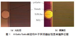
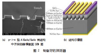
图1为AlGaAs/GaAs微结构中子探测器正面金相显微镜表征图,图1(a)、(b)分别是探测器光刻后以及电极沉积后的金相图,探测器为边长2 mm的正方形,有效面积4 mm2。将两份材料用丙酮、乙醇、去离子水清洗,通过光刻流程得到电极形状,用电子束、热蒸发镀膜机在上表面镀上Ti/Pt/Au(40 nm/20 nm/200 nm)的正方形欧姆接触电极,材料反面镀Ni/Ge/Au(50 nm/50 nm/425 nm)后快速退火形成欧姆接触电极。使用丙酮试剂作为剥离剂,清洗掉沟槽内部的电极,最后清洗吹干,得到制备好的探测器如图2所示。p-i-n型微结构Al⁃GaAs/GaAs中子探测器上表面欧姆接触工艺难度较大,微结构上的电极需要经过光刻、套刻,套刻时掩模版的图形需整齐掩盖在沟槽的上表面,裸露出沟槽上表面用来沉积金属,沟槽内部及侧壁用光刻胶阻挡。镀电极时沟槽不得有金属存在,否则p-i-n异质结会短路,导致整个微结构探测器报废。
AlGaAs/GaAs微结构中子探测器制备好后,将带有Ni/Ge/Au电极的一面使用纳米导电银浆连接在沉金PCB板上,使用金丝球焊机连接Ti/Pt/Au电极和PCB板。使用Keithley模型4200-SCS半导体表征系统来分析两种探测器的电学性质,对比平面结构和沟槽结构探测器的漏电流变化。为对比两种不同结构探测器的α粒子探测性能,实验使用Ortec核电子测量系统和能量为5.48 MeV的241Amα源测试两种探测器的脉冲高度谱,Ortec系统由电荷灵敏前置放大器142PC、成形放大器572A、多通道脉冲高度分析仪ASPEC-927组成。
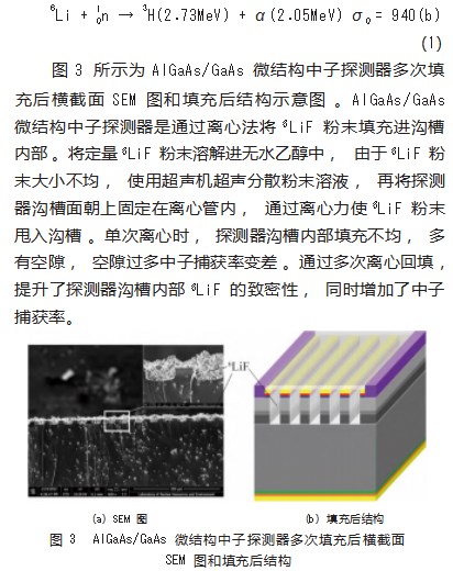
在测试完探测器的电学特性和α粒子能谱后,用241Am-Be快中子源作为实验中子探测源。由于快中子不带电且速度很快无法探测到,因此使用高密度聚乙烯将快中子慢化成热中子。将中子转换材料6LiF或10B4C涂覆在探测器表面,通过核反应法,热中子与转换材料反应产生带电粒子,带电粒子在探测器中电离从而被探测。10B4C具有较高的反应截面,但是反应产物的能量对于6LiF来说较低[13],因此选用6LiF作为中子转换材料。中子与6LiF转换材料的核反应方程式[14]如下:
2结果与讨论
2.1 I-V测试
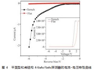
对于核辐射探测器而言,小的漏电流能够使探测器有更好的探测效率和更高的能量分辨率[15]。图4所示为平面型和微结构AlGaAs/GaAs探测器的电流-电压特性曲线。在相同电压条件下,微结构AlGaAs/GaAs探测器的漏电流大于平面型AlGaAs/GaAs探测器的漏电流。在-1 V时,平面型和微结构AlGaAs/GaAs探测器的漏电流分别是-1.3 nA、-33.1 nA。在-5 V时,平面型和微结构AlGaAs/GaAs探测器的漏电流分别是-0.024 1µA、-0.627µA,两者相差近30倍。材料表面刻蚀沟槽深度较深,刻穿了整个p-i-n AlGaAs/GaAs异质结结构,刻蚀沟槽使AlGaAs/GaAs材料的表面态发生变化,器件表面漏电流变大。
2.2 C-V测试
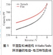
图5所示为平面型和微结构AlGaAs/GaAs探测器的电容-电压特性曲线,从图中可以看出,平面型和微结构的结电容都随偏压的增大而减小,这是由于反向偏压增大后,使探测器的耗尽区展宽导致结电容减小。在-5 V反偏电压下时,平面型和微结构AlGaAs/GaAs探测器的结电容分别是641.7 pF、587.4 pF。平面型结电容比微结构结电容略大,由于微结构探测器表面刻有较深的沟槽,改变了耗尽层原有的异质结结构,使得结电容变小,小的结电容反而有利于信号的收集。其电容与耗尽层宽度的表达式为[16]:
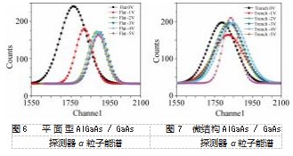
图6~7所示为平面型和微结构AlGaAs探测器在偏压0 V到-5 V下的α粒子能谱响应图。由图可以看出,随着偏压的增大,平面和微结构探测器的能谱峰位也随之增大。相较于平面探测器,微结构探测器的能谱分辨率和能谱计数均有不同程度的差别。平面AlGaAs/GaAs探测器在0 V偏压下时,能量分辨率为9.99%,随着偏压的增高,AlGaAs/GaAs探测器的耗尽区会随偏置电压的增大而展宽,展宽的耗尽区能接收更多α粒子产生的信号,使能谱峰位向高能端偏移,在-3 V偏压时具有最佳能谱分辨率6.13%;而后随着偏压增大,漏电流也逐渐变大,一些弱信号被大的漏电流所掩盖,能谱计数随之下降。微结构AlGaAs/GaAs探测器0 V偏压下能谱分辨率为11.08%,这是由于微结构AlGaAs/GaAs探测器在刻蚀沟槽时整体异质结结构被刻穿,导致探测器收集电子-空穴对效率变差,而偏压增大时能谱峰位向高能端偏移较小,在偏压-5 V时达到最佳分辨率为6.16%。在0 V偏压下,微结构与平面的结电容几乎相同,微结构由于异质结刻穿后信号收集面积比平面小,能谱计数低于平面。而在有偏压下,微结构的结电容比平面小,信号收集效率更高,能谱计数高于平面。
2.4中子测试
为测试微结构AlGaAs/GaAs探测器中子探测性能,准备了平面和微结构两种不同结构的中子探测器。填充好中子转换材料的探测器使用图3相同步骤连接起来,装入Ortec核电子测量系统中,将241Am-Be快中子源放入铅罐,加上适度高度的高密度聚乙烯材料漫化,将Ortec核电子测量系统连接,开始测试中子计数。本实验使用的中子源中子产额约为104n/s,中子241Am衰变产生的带电粒子轰击Be产生。图8~10所示为平面与微结构中子探测器不同偏压下的中子计数图。在600 s中子计数时间内,平面AlGaAs/GaAs中子探测器在0 V偏压下,测得的总中子计数为19个,微结构AlGaAs/GaAs中子探测器0 V偏压下的总中子计数为39个。微结构比平面型中子探测器中子总计数多1倍,这是由于微结构探测器的沟槽结构一方面增加了衬底与中子转化材料的接触面积,增大了探测器的对中子俘获效率;另一方面沟槽减小了中子转化材料的自吸收效应,增加了带电粒子进入探测器的概率。图9~10分别为微结构AlGaAs探测器0 V和5 V偏压下的中子计数,5 V偏压时600 s总计数为41个,与0 V偏压相比有些许提升,这是由于在偏压条件下,探测器的耗尽层展宽,增大了电子空穴对的收集概率。
3结束语
生长并制备了探测面积4 mm2、沟槽深度10µm的p-i-n型微结构AlGaAs/GaAs中子探测器,为对比平面与沟槽结构探测效率,制备了相同面积的平面AlGaAs/GaAs中子探测器。对比了两种不同结构探测器的电学特性和α粒子能谱响应,使用241Am-Be快中子源测试了两种结构的探测器的中子计数。由于刻蚀微结构刻穿了异质结结构,在电学测试和α粒子能谱响应中,微结构探测器的漏电流、电容以及α粒子能量分辨率均比平面探测器表现有较大差别。在对中子的测试中,微结构降低了探测器的自吸收效应而且增大了探测器与中子转换层的接触面积,进而增强了微结构探测器的中子探测能力。在填充中子转换层时,采用多次离心填充,降低了沟槽内部的存在空隙可能性,从而使沟槽充分发挥了结构的优势。微结构探测器探测中子的能力比平面强不少,在探测中子信号上,微结构探测器有广阔的应用前景。
参考文献:
[1]Eberhardt J E,Ryan R D,Tavendale A J.Evaluation of epitaxial n-GaAs for nuclear radiation detection[J].Nuclear Instruments and Methods,1971,94(3):463-476.
[2]Owens A,Peacock A.Compound semiconductor radiation detec⁃tors[J].Nuclear Instruments and Methods in Physics Research Section A:Accelerators,Spectrometers,Detectors and Associat⁃ed Equipment,2004,531(1-2):18-37.
[3]Eberhardt J E,Ryan R D,Tavendale A J.High⁃Resolution Nucle⁃ar Radiation Detectors From Epitaxial n⁃GaAs[J].Applied Phys⁃ics Letters,1970,17(10):427-429.
[4]McGregor D S,Klann R T,Gersch H K,et al.Thin-film-coated bulk GaAs detectors for thermal and fast neutron measurements[J].Nuclear Instruments and Methods in Physics Research Sec⁃tion A:Accelerators,Spectrometers,Detectors and Associated Equipment,2001,466(1):126-141.
[5]邓文娟,朱斌,王壮飞,等.变掺杂变组分AlxGa1–xAs/GaAs反射式光电阴极分辨力特性[J].物理学报,2022,71(15):271-277.
[6]Diao Y,Liu L,Xia S.Photon-enhanced thermionic emission so⁃lar energy converters with GaAs wire array cathode under exter⁃nal electric field[J].Applied Nanoscience,2020,10(3):807-817.
[7]Silenas A.Graded-gap AlxGa1−xAs analyzer of X-ray and alpha-particle spectra[J].Nuclear Instruments and Methods in Physics Research Section A:Accelerators,Spectrometers,Detectors and Associated Equipment,2004,531(1-2):92-96.
[8]Zhu Z F,Zou J J,Sun Z J,et al.Graded composition and doping pin AlxGa1−xAs/GaAs detector for unbiased voltage operation[J].Nuclear Science and Techniques,2022,33(7):1-10.
[9]ŠagátováA,Zat'ko B,SedlačkováK,et al.Semi-insulatingGaAs detectors optimized for fast neutron detection[J].Journal of Instrumentation,2013,8(3):C03016.
[10]Chernykh A V,Chernykh S V,Didenko S I,et al.Fast neutron detector based on surface-barrier VPE GaAs structures[J].Jour⁃nal of Instrumentation,2015,10(1):C01021.
[11]Muminov R A,Tsvang L D.High-efficiency semiconductor theramal-neutron detectors[J].Soviet Atomic Energy,1987,62(4):316-319.
[12]McGregor D S,Klann R T,Gersch H K,et al.New surface mor⁃phology for low stress thin-film-coated thermal neutron detec⁃tors[J].IEEE Transactions on Nuclear Science,2002,49(4):1999-2004.
[13]V Mclane,Dunford C L.Neutron Cross Sections:Neutron Cross Section Curves[M].San Diego,Academic Press,2012.
[14]McGregor D S,Hammig M D,Yang Y H,et al.Design consider⁃ations for thin film coated semiconductor thermal neutron detec⁃tors—I:basics regarding alpha particle emitting neutron reac⁃tive films[J].Nuclear Instruments and Methods in Physics Re⁃search Section A:Accelerators,Spectrometers,Detectors and Associated Equipment,2003,500(1-3):272-308.
[15]Zhu Z F,Peng X C,Zou J J,et al.A Study on the Electrical Properties of GaN-based Alpha Particle Detector[C]//Applied Mechanics and Materials.Trans Tech Publications Ltd,2014,620:457-460.
[16]Zhao S,Lioliou G,Barnett A M.X-ray spectrometer with a low-cost SiC photodiode[J].Nuclear Instruments and Methods in Physics Research Section A:Accelerators,Spectrometers,De⁃tectors and Associated Equipment,2018,887:138-143.
[17]Ng B K,David J P R,Plimmer S A,et al.Avalanche multiplica⁃tion characteristics of Al/sub 0.8/Ga/sub 0.2/As diodes[J].IEEE Transactions on Electron Devices,2001,48(10):2198-2204.
关注SCI论文创作发表,寻求SCI论文修改润色、SCI论文代发表等服务支撑,请锁定SCI论文网!
文章出自SCI论文网转载请注明出处:https://www.lunwensci.com/ligonglunwen/56524.html